


Ηλεκτρονικό Μικροσκόπιο TEM
Transmission electron microscopy (TEM) is a powerful tool for examining materials at high resolution.In the microscope, electrons are directed through a series of lenses through a thin sample (<200 nm thick).TEM can provide microstructural details down to an atomic level and can be utilised to examine crystal structures and crystalline defects.
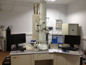
The JEM-2100 is an advanced Field Emission Electron Microscope featuring ultrahigh resolution and rapid data acquisition. The JEM 2100 is a next generation TEM that simplifies atomic level structural analyses in biology, medicine, and materials sciences as well as the semiconductor and pharmaceutical industries.
Transmission electron microscopy (TEM) is a powerful tool for examining materials at high resolution. In the microscope, electrons are directed through a series of lenses through a thin sample (<200 nm thick). The transmitted electrons then pass through additional lenses to be projected onto a viewing screen or recorded with a digital camera. TEM can provide microstructural details down to an atomic level and can be utilised to examine crystal structures and crystalline defects.
The JEM-2100 has been developed to achieve the highest image quality and the highest analytical performance in the 200kV class analytical TEM with a probe size under 0.5nm. The new side-entry goniometer stage provides ease of use tilt, rotation, heating and cooling, programmable multi-point settings–all without mechanical drift. The JEM-2100 equipped with EDS and CCD-cameras.
TEM is one of the first non optical microscopes developed, initially to overcome the resolution limit of light microscopes. After development, it was discovered that electron microscopes have many addition benefits, including better depth of view. As the name suggests, in TEM, electrons transmit through a thin sample. As they pass through the sample, some of the electrons interact with the sample (atom based electrons) through elastic scattering, and are forward scattered towards a fluorescent screen (or suitable camera) where they are detected. This scattering by atoms in the specimen perturb the plain coherent wave of electrons impinging on the specimen and enables us to image features on the sample at high resolutions.
JEM 2100 TEM in our laboratory.
The JEM 2100 TEM is a high resolution (x300 – x1.5M) 200kV TEM, with electron diffraction, two Gatan cameras for digital image capture and an Oxford Instruments EDS system for elemental analysis. The system is complimented with a gatan TEM sample preparation system, including a precision ion polishing system.
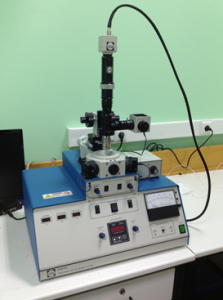
Precision Ion Polishing System in our sample-prep room.
Relevant Links
TEM on Wikipedia
Electron Microscopy in Nanoscience
JEM 2100 TEM